From 800G backbone optical transceivers and 6G mmWave front-ends to automotive LiDAR and frontier quantum devices, InP is defining the boundaries of next-generation semiconductors.

High-speed optical transceivers for AI data centers (800G/1.6T/CPO), long-haul fiber transmission, and 5G/6G optical fronthaul; used for DFB lasers, EML modulators, photodetectors, and photonic integrated circuits (PIC), compatible with the 1310/1550 nm fiber communication windows.
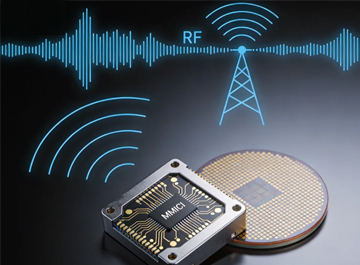
InP HEMT/HBT high-frequency transistors with low noise and high electron mobility; used in LEO satellite payloads, on-board RF amplifiers, mmWave communication, airborne phased-array radar, and electronic warfare, with strong radiation tolerance for space environments.
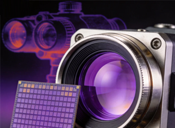
Focused on 1550 nm eye-safe automotive LiDAR, plus space laser communication, ranging, infrared detection, and single-photon detection; the mainstream substrate solution for high-end LiDAR light sources and receiver chips.
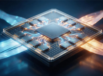
Space-grade high-efficiency multi-junction solar cells (space photovoltaics), plus quantum photonics (QKD, single-photon sources), terahertz imaging and inspection, and other frontier research and specialty equipment applications.
Filter InP substrates by size, doping, and resistivity, with real-time specifications and availability.
From cleanroom facilities and a specialized team to volume yield and quality systems, we deliver stable, reliable industrialization for InP substrate manufacturing.

16,000 m² semiconductor cleanroom with ultrapure water treatment, meeting the stringent process environment requirements of compound semiconductor wafer manufacturing.
A senior team with deep experience in compound semiconductors and wafer equipment; R&D staff account for over 40%, with 20+ years of average industry experience.
Stable high-volume substrate production lines running at 300,000 wafers per year, with industry-leading batch consistency and yield.
ISO 9001 / ISO 14001, approved under customer qualified supplier systems, with full-process quality traceability.
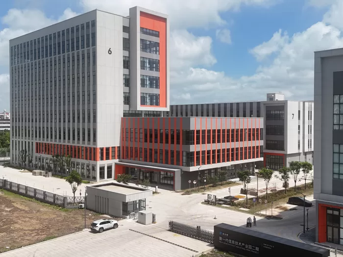
Jiangsu Xinguang Yuan Crystal Technology Co., Ltd.(Synlumin) is located in Qidong, Nantong, Jiangsu, the core hinterland of the semiconductor industry in the Yangtze River Delta region. The company focuses on the localization needs of compound semiconductor materials and specializes in the research, development, production, and sales of indium phosphide (InP) substrates and epitaxial materials.
The company's main business covers 2/3/4/6 inch InP single crystal substrates and provides customized and joint development services. The products are widely used in cutting-edge fields such as optical communication, RF devices, infrared detection, and quantum information.
Company news, product launches, and industry insights, keeping you up to date on our latest InP developments.
The material of choice for high-speed optical communication, AI data center interconnects, and advanced sensing applications.
Tell us your requirements and our technical team will respond within one business day with samples and customized solutions.